Audio Amplifier
Contents
Overview
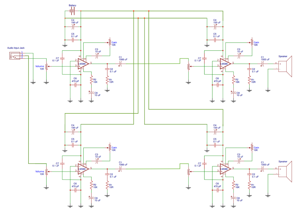
In this project, we will develop a prototype of a dual-channel audio amplifier with independent volume control in each channel based on operational amplifiers. An operational amplifier is a voltage amplifying device designed to be used with external feedback components such as capacitors and resistors between the output and input terminals. In the prototype, the operational amplifiers take an audio input signal and increase its potential. Gain is a characteristic of the amplifier that can set the range of possible volume levels. Volume is the sound level adjustment within the range of amplification set by the gain. For the design, we are going to make the design with more stability and less noise and distortion.
Background
In order to work on this project, you need certain ECE knowledge background. Please read and learn the following content slowly and carefully. Operational Amplifier (Op-Amp) An operational amplifier (often op-amp or opamp) is a DC-coupled high-gain electronic voltage amplifier with a differential input and, usually, a single-ended output. It is also a device that realizes two blocks of the negative feedback system, including the difference block and the high gain block. The popularity of the op-amp as a building block in analog circuits is due to its versatility. With negative feedback, the characteristics of an op-amp circuit, gain, bandwidth, input, and output impedance are determined by external components and have little dependence on temperature coefficients or engineering tolerance in the op-amp itself. In the audio amplifier design, we are going to use negative feedback. For applications of the operational amplifier, precision control, one of the key aspects of audio system design, would be impossible without negative feedback.
Amplifier Classes Not all amplifiers are the same, and there is a clear distinction made between the way their output stages are configured and operated. The main operating characteristics of an ideal amplifier are linearity, signal gain, efficiency, and power output, but in real-world amplifiers, there is always a trade-off between these different characteristics. Generally, large signal or power amplifiers are used in the output stages of audio amplifier systems to drive a loudspeaker load. A typical loudspeaker has an impedance of between 4Ω and 8Ω. Thus a power amplifier must be able to supply the high peak currents required to drive the low impedance speaker. One method used to distinguish the electrical characteristics of different types of amplifiers is by “class,” and as such, amplifiers are classified according to their circuit configuration and method of operation. Then Amplifier Classes is the term used to differentiate between the different amplifier types.
Class A Amplifier
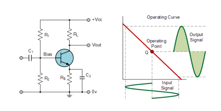
Class A Amplifiers are the most common type of amplifier topology as they use just one output switching transistor within their amplifier design. This single output transistor is biased around the Q-point within the middle of its load line and so is never driven into its cut-off or saturation regions, thus allowing it to conduct current over the full 360 degrees of the input cycle. Then the output transistor of a class-A topology never turns off, which is one of its main disadvantages.
Class “A” amplifiers are considered the best class of amplifier design due mainly to their excellent linearity, high gain, and low signal distortion levels when designed correctly. Although seldom used in high-power amplifier applications due to thermal power supply considerations, class-A amplifiers are probably the best sounding of all the amplifier classes mentioned here and as such, are used in high-fidelity audio amplifier designs.
Figure 1: Class A Amplifier
To achieve high linearity and gain, the output stage of a class A amplifier is biased “ON” all the time. Then for an amplifier to be classified as “Class A,” the zero signal idle current in the output stage must be equal to or greater than the maximum load current required to produce the largest output signal.
As a class A amplifier operates in the linear portion of its characteristic curves, the single output device conducts through a full 360 degrees of the output waveform. Then the class A amplifier is equivalent to a current source.
Since a class A amplifier operates in the linear region, the transistor’s base DC biasing voltage should be chosen properly to ensure correct operation and low distortion. However, as the output device is “ON” at all times, it constantly carries current, which represents a continuous loss of power in the amplifier.
Due to this continuous loss of power, class A amplifiers create tremendous amounts of heat, adding to their very low efficiency at around 30%, making them impractical for high-power amplification. Also, due to the high idling current of the amplifier, the power supply must be sized accordingly and be well filtered to avoid any amplifier hum and noise. Therefore, more efficient amplifier classes have been developed due to the low efficiency and overheating problems of Class A amplifiers.
Class B Amplifier
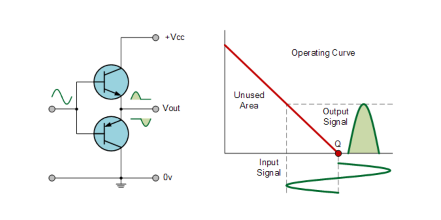
Class B amplifiers were invented to solve the efficiency and heating problems associated with the previous class A amplifier. The basic class B amplifier uses two complementary transistors, bipolar or FET, for each half of the waveform with its output stage configured in a “push-pull” type arrangement so that each transistor device amplifies only half of the output waveform.
In the class B amplifier, there is no DC base bias current as its quiescent current is zero, so the dc power is small, and therefore its efficiency is much higher than that of the class A amplifier. However, the price paid for the improvement in efficiency is in the linearity of the switching device.
Figure 2: Class B Amplifier
When the input signal goes positive, the positively biased transistor conducts while the negative transistor is switched “OFF.” Likewise, when the input signal goes negative, the positive transistor switches “OFF” while the negatively biased transistor turns “ON” and conducts the negative portion of the signal. Thus the transistor conducts only half of the time, either on the positive or negative half cycle of the input signal. Then we can see that each transistor device of the class B amplifier only conducts through one half or 180 degrees of the output waveform in strict time alternation, but as the output stage has devices for both halves of the signal waveform, the two halves are combined together to produce the full linear output waveform. This push-pull design of amplifier is obviously more efficient than Class A, at about 50%, but the problem with the class B amplifier design is that it can create distortion at the zero-crossing point of the waveform due to the transistors dead band of input base voltages from -0.7V to +0.7. It takes a base-emitter voltage of about 0.7 volts to get a bipolar transistor to start conducting. Then in a class B amplifier, the output transistor is not “biased” to an “ON” state of operation until this voltage is exceeded. This means that the part of the waveform which falls within this 0.7-volt window will not be reproduced accurately, making the class B amplifier unsuitable for precision audio amplifier applications. Class AB amplifiers were developed to overcome this zero-crossing distortion, which is also known as Crossover Distortion.
Class AB Amplifier
As its name suggests, the Class AB Amplifier is a combination of the “Class A” and the “Class B” type amplifiers we have looked at above. The AB classification of the amplifier is currently one of the most commonly used types of audio power amplifier design. The class AB amplifier is a variation of a class B amplifier as described above, except that both devices are allowed to conduct at the same time around the waveforms crossover point, eliminating the crossover distortion problems of the previous class B amplifier.
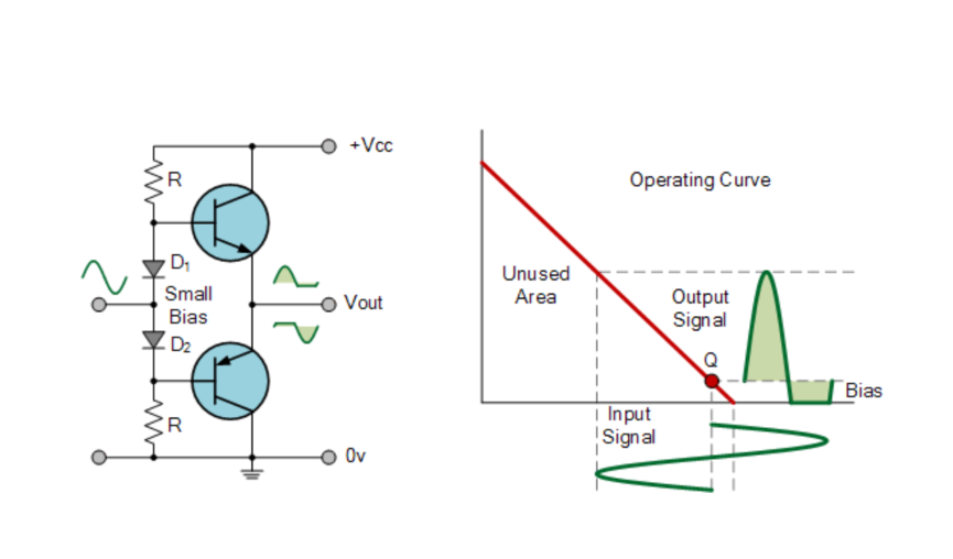
The two transistors have a very small bias voltage, typically at 5 to 10% of the quiescent current, to bias the transistors just above their cut-off point. Then the conducting device, either bipolar or FET, will be “ON” for more than one-half cycle but much less than one full cycle of the input signal. Therefore, in a class AB amplifier design, each of the push-pull transistors is conducting for slightly more than the half cycle of conduction in class B but much less than the full cycle of conduction in class A.
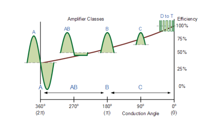
In other words, the conduction angle of a class AB amplifier is somewhere between 180oand 360o depending upon the chosen bias point, as shown.
Figure 3: Class AB Amplifier
The advantage of this small bias voltage, provided by series diodes or resistors, is that the crossover distortion created by the class B amplifier characteristics is overcome without the inefficiencies of the class A amplifier design. So the class AB amplifier is a good compromise between class A and class B in terms of efficiency and linearity, with conversion efficiencies reaching about 50% to 60%.
Due to its heavy audio distortion, class C amplifiers are commonly used in high-frequency sine wave oscillators and certain types of radio frequency amplifiers, where the pulses of the current produced at the output of the amplifier can be converted to complete sine waves of a particular frequency by the use of LC resonant circuits in its collector circuit.
Amplifier Class Summary
The quiescent DC operating point (Q-point) of an amplifier, determines the amplifier classification. By setting the position of the Q-point at halfway on the load line of the amplifier’s characteristics curve, the amplifier will operate as a class A amplifier. Moving the Q-point lower down the load line changes the amplifier into a class AB, B, or C amplifier.
Figure 4: Amplifier Class Summary
As well as audio amplifiers, there are a number of high-efficiency Amplifier Classes relating to switching amplifier designs that use different switching techniques to reduce power loss and increase efficiency. Some amplifier class designs listed below use RLC resonators or multiple power-supply voltages to reduce power loss or are digital DSP (digital signal processing) type amplifiers that use pulse width modulation (PWM) switching techniques.
Negative Feedback Feedback is the process by which a fraction of the output signal, either a voltage or a current, is used as an input. If this feedback fraction is opposite in value or phase, which is “anti-phase”, to the input signal, then the feedback is said to be negative feedback or degenerative feedback. Negative feedback opposes or subtracts from the input signals giving it many advantages in the design and stabilization of control systems. For example, if the output of the system changes for any reason, then negative feedback affects the input in such a way as to counteract the change. Feedback reduces the overall gain of a system, with the degree of reduction being related to the system’s open-loop gain. Negative feedback also has effects of reducing distortion, noise, and sensitivity to external changes as well as improving system bandwidth and input and output impedances.
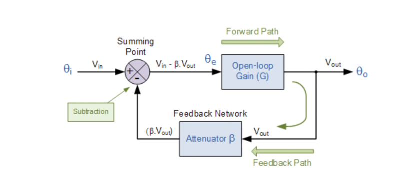
Feedback in an electronic system, whether negative feedback or positive feedback, is unilateral in direction. Meaning that its signals flow one way only from the output to the input of the system. This then makes the loop gain, G of the system, independent of the load and source impedances. As feedback implies a closed-loop system, it must therefore have a summing point. In a negative feedback system, this summing point or junction at its input subtracts the feedback signal from the input signal to form an error signal, β which drives the system. If the system has a positive gain, the feedback signal must be subtracted from the input signal in order for the feedback to be negative, as shown.
Figure 5: Negative Feedback circuit
The circuit shown above represents a system with positive gain, G, and negative feedback, β. The summing junction at its input subtracts the feedback signal from the input signal to form the error signal Vin – βG, which drives the system.
Capacitors
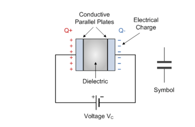
Capacitors are energy storage devices that have the ability to store an electrical charge across their plates. Thus capacitors store energy as a result of their ability to store charge, and an ideal capacitor would not lose its stored energy. The simplest construction of a capacitor is by using two parallel conducting metal plates separated through a distance by an insulating material called the dielectric.
In audio system design, capacitors are used to separate DC from AC signals -- basically bias from audio. They are also used to adjust the frequency response in case it is needed to compensate for imperfections in other devices. They are also used to filter noises, including ripple from the supply, or act as small 'backups' for large surges of power.
Figure 6: Capacitor structure and symbol
Resistors in AC Circuits
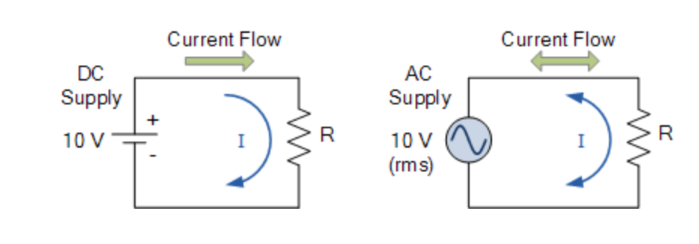
Resistors are “passive” devices, that is they do not produce or consume any electrical energy but convert electrical energy into heat. In DC circuits the linear ratio of voltage to current in a resistor is called its resistance. However, in AC circuits this ratio of voltage to current depends upon the frequency and phase difference or phase angle (φ) of the supply. So when using resistors in AC circuits the term Impedance, symbol Z is generally used, and we can say that DC resistance = AC impedance, R = Z. It is important to note that when used in AC circuits, a resistor will always have the same resistive value no matter what the supply frequency from DC to very high frequencies, unlike capacitors and inductors. For resistors in AC circuits, the direction of the current flowing through them has no effect on the behavior of the resistor, so it will rise and fall as the voltage rises and falls. The current and voltage reach maximum, fall through zero, and reach a minimum simultaneously. The rise and fall simultaneously are said to be “in-phase”. In purely resistive series AC circuits, all the voltage drops across the resistors can be added together to find the total circuit voltage as all the voltages are in-phase. Likewise, in a purely resistive parallel AC circuit, all the individual branch currents can be added together to find the total circuit current because all the branch currents are in-phase. Since for resistors in AC circuits, the phase angle φ between the voltage and the current is zero, then the power factor of the circuit is given as cos (0) = 1.0. The power in the circuit at any instant in time can be found by multiplying the voltage and current at that instant.
Figure 7: Resistors in DC and AC supplies
Some resources:
E Term 2022 Project
The goal of this project is to 1) understand the principle of amplifier 2) design the circuits. 3)build and debug the prototype.
Starting Point
The immediate objective for this term is to design and build our amplifier including:
- Buying materials for future use.
- Pick and test speakers.
- Design the circuit.
- Build and test our prototype.
Guiding Questions:
- What kind of amplifier works better?
- What would affect the quality of sound?
- What kind of output we can get?
Results
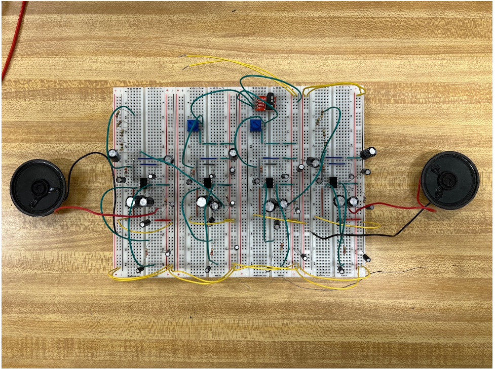
Figure 8: Final Circuit Design
And we recorded a video for future participants [2]
Future Goals/Recommendations
During the week before the deadline, we tried to improve the design of the audio amplifier prototype with LM386; for instance, we replaced a speaker with better sound quality(same impedance, higher wattage), and bigger capacitor at the output of the second-stage amplifier. The sound quality of the prototype got better, even though it still couldn’t handle the MP3 source with more tracks from different musical instruments. Unfortunately, most of the LM386 IC burnt out during testing. Even though the result was not satisfying, we finished the prototype and found directions for the next step of this audio amplifier design.
1)If the sound quality is not the top priority, we can make the circuit design into PCB, and design the package for speakers. 2)(Highly recommended) If the sound quality is the top priority, find better ICs for the prototype design.
Project Files & Resources
Documentation
WPI Student Contributors
2022
- Haoyu Fu
- Qing(Jim) Huang
